
Analytical Model for Electronic Transport in Semiconductor Thin Films
Main Article Content
Keywords
Thin films, semiconductors, electrical Conduction, Model.
Abstract
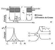
Polycrystalline semiconductors are materials who often exhibit unusual electrical properties. In the model we assume that the crystals are composed of semiconductor material, the grain itself, which is surrounded by highly disordered and resistive materials, the grain boundary. The grain boundary disturbs the structural regularity of the crystal giving rise to localized electronic states within the energy gap. The existence of these states promotes the charge trapping at the grain boundaries and the bending of the energy bands. This bending is characterized by a potential barrier and a space charge zone which control the electron transport through the grain boundary. The model uses the diusion and drift carriers theories, and thermoionic emission, and the quantum tunneling of carriers through the potential barrier was also taken into consideration. Since the structure of the thin lms of molybdenum trioxide (MoO3) obtained through spray pyrolysis is granular and nanosize, the model described the behavior of the current-voltage characteristic (I-V) of the films.
PACS: 73.25.+i, 73.50.Gr, 73.61.Cw
MSC: 74K35, 82D37, 03C90
Downloads
References
[2] J. P. Meyer, D. Schlettwein, D. Wohrle, and N. I. Jaeger, ''Charge transport in thin films of molecular semiconductors as investigated by measurements of thermoelectric power and electrical conductivity,'' Thin Solid Films, vol. 258, no. 1–2, pp. 317–324, 1995.
[3] J. López-García, J. F. Trigo, I. J. Ferrer, C. Guillén, and J. Herrero, ''CuAlxGa1-xSe2 thin films for photovoltaic applications: Structural, electrical and morphological analysis,'' Materials Research Bulletin, vol. 47, no. 9, pp. 2518–2524, 2012.
[4] A. Sharma, M. Tomar, and V. Gupta, ''SnO2 thin film sensor with enhanced response for NO2 gas at lower temperatures,'' Sensors and Actuators B: Chemical, vol. 156, no. 2, pp. 743–752, 2011.
[5] E. Brunet, T. Maier, G. C. Mutinati, S. Steinhauer, A. Kock, C. Gspan, and W. Grogger, ''Comparison of the gas sensing performance of SnO2 thin film and SnO2 nanowire sensors,'' Sensors and Actuators B: Chemical, vol. 165, no. 1, pp. 110–118, 2012.
[6] Z. M. Seeley, A. Bandyopadhyay, and S. Bose, ''Titanium dioxide thin films for high temperature gas sensors,'' Thin Solid Films, vol. 519, no. 1, pp. 434–438, 2010.
[7] Q. Liang, H. Xu, J. Zhao, and S. Gao, ''Micro humidity sensors based on ZnO-In2O3 thin films with high performances,'' Sensors and Actuators B: Chemical, vol. 165, no. 1, pp. 76–81, 2012.
[8] J. A. Park, J. Moon, S. J. Lee, S. Hyun-Kim, H. Yong-Chu, and T. Zyung, ''SnO2-ZnO hybrid nanofibers-based highly sensitive nitrogen dioxides sensor,'' Sensors and Actuators B: Chemical, vol. 145, no. 1, pp. 592–595, 2010.
[9] N. Van Hieu, N. A. P. Duc, T. Trung, M. A. Tuan, and N. D. Chien, ''Gassensing properties of tin oxide doped with metal oxides and carbon nanotubes,'' Sensors and Actuators B: Chemical, vol. 144, no. 2, pp. 450–456, 2010.
[10] T. S.Wang, Q. S.Wang, C. L. Zhu, Q. Y. Ouyang, L. H. Qi, C. Y. Li, G. Xiao, P. Gao, and Y. J. Chen, ''Gas-sensing properties of tin oxide doped with metal oxides and carbon nanotubes,'' Sensors and Actuators B: Chemical, vol. 171–172, no. 1, pp. 256–262, 2012.
[11] M. B. Rahmani, S. H. Keshmiri, J. Yu, A. Z. Sadek, L. Al-Mashat, A. Moafi, K. Latham, Y. X. Li, W. Wlodarski, and K. Kalantar-Zadeh, ''Gas sensing properties of thermally evaporated lamellar MoO3,'' Sensors and Actuators B: Chemical, vol. 145, no. 1, pp. 13–19, 2010.
[12] J. Zeng, M. Hu, W. Wang, H. Chen, and Y. Qin, ''NO2-sensing properties of porous WO3 gas sensor based on anodized sputtered tungsten thin film,'' Sensors and Actuators B: Chemical, vol. 161, no. 1, pp. 447–452, 2010.
[13] P. Gao, H. Ji, Y. Zhou, and X. Li, ''Selective acetone gas sensors using porous WO3-Cr2O3 thin films prepared by sol-gel method,'' Thin Solid Films, vol. 520, no. 7, pp. 3100–3106, 2012.
[14] T. Samerjai, N. Tamaekong, C. Liewhiran, A. Wisitsoraat, A. Tuantranont, and S. Phanichphant, ''Selectivity towards H2 gas by flame-made Pt-loaded WO3 sensing films,'' Sensors and Actuators B: Chemical, vol. 157, no. 1, pp. 290–297, 2011.
[15] Y. C. Chen, T. C. Chang, H. W. Li, W. F. Chung, S. C. Chen, C. P. Wu, Y. H. Chen, Y. H. Tai, T. Y. Tseng, and F. S. Yeh(Huang), ''Characterization of environment-dependent hysteresis in indium gallium zinc oxide thin film transistors. Surface and Coatings Technology,'' Surface and Coatings Technology, vol. 231, pp. 531–534, 2012.
[16] V. K. Gueorguiev, P. V. Aleksandrova, T. E. Ivanov, and J. B. Koprinarova, ''Hysteresis in metal insulator semiconductor structures with high temperature annealed ZrO2/SiOx layers,'' Thin Solid Films, vol. 517, no. 5, pp. 1815–1820, 2009.
[17] E. Lee, J. M. Lee, J. H. Koo, W. Lee, and T. Lee, ''Hysteresis behavior of electrical resistance in Pd thin films during the process of absorption and desorption of hydrogen gas,'' International Journal of Hydrogen Energy, vol. 35, no. 13, pp. 6984–6991, 2010.
[18] A. Varpula, J. Sinkkonen, and S. Novikov, ''Modelling of dc characteristics for granular semiconductors,'' Physica Scripta, vol. T141, no. 014003, pp. 1–4, 2010.
[19] A. Varpula, J. Sinkkonen, and S. Novikov, ''Small-signal analysis of granular semiconductors,'' Physica Scripta, vol. T141, no. 014002, pp. 1–4, 2010.
[20] A. Pardo and J. Torres, ''Substrate and annealing temperature effects on the crystallographic and optical properties of MoO3 thin films prepared by laser assisted evaporation,'' Thin Solid Films, vol. 520, no. 6, pp. 1709–1717, 2012.
[21] H. M. Martínez, J. Torres, L. D. López-Carreño, and M. E. Rodríguez-García, ''The Effect of substrate Temperature on the Optical Properties of MoO3 Nano-crystals prepared using spray pyrolysis,'' Journal of Superconductivity and Novel Magnetism, vol. 26, no. 7, pp. 2485–2488, 2012.
[22] Y. A. Pastrana, J. Torres, L. D. López-Carreño, and H. M. Martínez, ''The influence of oxygen on the structural and optical properties of MoO3 thin films prepared using the laser-assisted evaporation technique,'' Journal of Superconductivity and Novel Magnetism, vol. 26, no. 7, pp. 2475–2478, 2013.
[23] H. M. Martínez, J. Torres, M. E. Rodríguez-García, and L. D. López-Carreño, ''Gas sensing properties of nanostructured MoO3 thin films prepared by spray pyrolysis,'' Physica B, vol. 407, no. 16, pp. 3199–3202, 2012.
[24] H. M. Martínez, J. Torres, A. Pardo, L. C. Moreno, J. E. Alfonso, and L. D. López-Carreño, ''Películas delgadas de α-MoO3 preparadas por atomización pirolítica,'' Ingeniería y Ciencia, vol. 7, no. 14, pp. 105–117, 2011.
[25] J. M. Marshall, ''Carrier diffusion in amorphous semiconductors,'' Reports on Progress in Physics, vol. 46, no. 10, pp. 1235–1282, 1983.
[26] N. Barsan and U. Weimar, ''Conduction model of metal oxide gas sensor,'' Journal of Electroceramics, vol. 7, no. 3, pp. 143–147, 2001.
[27] N. Yamazoe, K. Shimanoe, and Y. Sawada, ''Contribution of electron tunneling transport in semiconductor gas sensor,'' Thin Solid Films, vol. 515, no. 23, pp. 8302–8309, 2007.
[28] H. Nemoto and I. Oda, ''Direct Examinations of PTC Action of Single Grain Boundaries in Semiconducting BaTiO3 Ceramic,'' Journal of the American Ceramic Society, vol. 63, no. 7–8, pp. 398–401, 1980.
[29] L. L. Kazmerski, Ed., Polycrystalline and Amorphous Thin and Films and Devices. New York: Academic Press, 1980.
[30] E. H. Rhoderick and R. H. Williams, Eds., Metal-Semiconductor Contacts. Oxford: Clarendon Press, 1988.
[31] W. A. Harrison, ''Tunneling from an Independent-Particle Point of View,'' Physical Review, vol. 123, no. 1, pp. 85–89, 1961.
[32] F. A. Padovani and R. Stratton, ''Field and Thermionic-Field.Emission in Schottky Barriers,'' Solid-State Electronics, vol. 9, no. 7, pp. 695–707, 1966.
[33] C. R. Crowell and V. L. Rideout, ''Normalized thermionic-field (T-F) emission in metal-semiconductor (Schottky) barriers,'' Solid-State Electronics, vol. 12, no. 2, pp. 89–105, 1969.
[34] S. M. Sze, Ed., Physics of Semiconductor Devices. New York: Wiley- Interscience, 1969.
[35] H. M. Martínez, J. Torres, L. D. López-Carreño, and M. E. Rodríguez-García, ''Effect of the substrate temperature on the physical properties of molydenum trioxide thin films obtained through the spray pyrolysis technique,'' Materials Characterization, vol. 75, pp. 184–193, 2013.
Article Sidebar
Article Details
M Torres-Luengo, Universidad Nacional de Colombia
FísicoH M Martínez, Universidad Nacional de Colombia
MSc.J Torres, Universidad Nacional de Colombia
Dr.Sc.L D López-Carreño, Universidad Nacional de Colombia
Dr.Sc.Authors who publish with this journal agree to the following terms:
- Authors retain copyright and grant the journal right of first publication with the work simultaneously licensed under a Creative Commons Attribution License that allows others to share the work with an acknowledgement of the work's authorship and initial publication in this journal.
- Authors are able to enter into separate, additional contractual arrangements for the non-exclusive distribution of the journal's published version of the work (e.g., post it to an institutional repository or publish it in a book), with an acknowledgement of its initial publication in this journal.
- Authors are permitted and encouraged to post their work online (e.g., in institutional repositories or on their website) prior to and during the submission process, as it can lead to productive exchanges, as well as earlier and greater citation of published work (See The Effect of Open Access).