
Modelo analítico para el transporte electrónico en películas delgadas semiconductoras
Main Article Content
Keywords
Semiconductores, Conducción eléctrica, modelo
Resumen
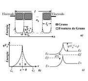
Los semiconductores policristalinos son materiales que a menudo presentan propiedades eléctricas inusuales. En el modelo se supone que los cristales están formados por material semiconductor, el grano en sí, el cual está rodeado por material altamente desordenado y resistivo, la frontera de grano. La frontera de grano perturba la periodicidad estructural del cristal dando origen a estados electrónicos localizados en el interior de la brecha de energía prohibida. La existencia de estos estados favorece el atrapamiento de carga en las fronteras de grano y al doblamiento de las bandas de energía. Este doblamiento se caracteriza por un potencial de barrera y una zona de carga espacial, las cuales gobiernan el transporte electrónico a través de la frontera de grano. El modelo utiliza las teorías de difusión y deriva de portadores, de emisión termoiónica e incluye además, la teoría de tunelamiento cuántico de portadores a través de la barrera de potencial. Dado que la estructura de las películas delgadas de trióxido de Molibdeno (MoO3) obtenidas por atomización pirolítica es de tipo granular y de tamaño nanométrico, el modelo analítico explica el comportamiento de la característica Corriente - Voltaje (I-V) de las películas.
PACS: 73.25.+i, 73.50.Gr, 73.61.Cw
MSC: 74K35, 82D37, 03C90
Descargas
Referencias
[2] J. P. Meyer, D. Schlettwein, D. Wohrle, and N. I. Jaeger, ''Charge transport in thin films of molecular semiconductors as investigated by measurements of thermoelectric power and electrical conductivity,'' Thin Solid Films, vol. 258, no. 1–2, pp. 317–324, 1995.
[3] J. López-García, J. F. Trigo, I. J. Ferrer, C. Guillén, and J. Herrero, ''CuAlxGa1-xSe2 thin films for photovoltaic applications: Structural, electrical and morphological analysis,'' Materials Research Bulletin, vol. 47, no. 9, pp. 2518–2524, 2012.
[4] A. Sharma, M. Tomar, and V. Gupta, ''SnO2 thin film sensor with enhanced response for NO2 gas at lower temperatures,'' Sensors and Actuators B: Chemical, vol. 156, no. 2, pp. 743–752, 2011.
[5] E. Brunet, T. Maier, G. C. Mutinati, S. Steinhauer, A. Kock, C. Gspan, and W. Grogger, ''Comparison of the gas sensing performance of SnO2 thin film and SnO2 nanowire sensors,'' Sensors and Actuators B: Chemical, vol. 165, no. 1, pp. 110–118, 2012.
[6] Z. M. Seeley, A. Bandyopadhyay, and S. Bose, ''Titanium dioxide thin films for high temperature gas sensors,'' Thin Solid Films, vol. 519, no. 1, pp. 434–438, 2010.
[7] Q. Liang, H. Xu, J. Zhao, and S. Gao, ''Micro humidity sensors based on ZnO-In2O3 thin films with high performances,'' Sensors and Actuators B: Chemical, vol. 165, no. 1, pp. 76–81, 2012.
[8] J. A. Park, J. Moon, S. J. Lee, S. Hyun-Kim, H. Yong-Chu, and T. Zyung, ''SnO2-ZnO hybrid nanofibers-based highly sensitive nitrogen dioxides sensor,'' Sensors and Actuators B: Chemical, vol. 145, no. 1, pp. 592–595, 2010.
[9] N. Van Hieu, N. A. P. Duc, T. Trung, M. A. Tuan, and N. D. Chien, ''Gassensing properties of tin oxide doped with metal oxides and carbon nanotubes,'' Sensors and Actuators B: Chemical, vol. 144, no. 2, pp. 450–456, 2010.
[10] T. S.Wang, Q. S.Wang, C. L. Zhu, Q. Y. Ouyang, L. H. Qi, C. Y. Li, G. Xiao, P. Gao, and Y. J. Chen, ''Gas-sensing properties of tin oxide doped with metal oxides and carbon nanotubes,'' Sensors and Actuators B: Chemical, vol. 171–172, no. 1, pp. 256–262, 2012.
[11] M. B. Rahmani, S. H. Keshmiri, J. Yu, A. Z. Sadek, L. Al-Mashat, A. Moafi, K. Latham, Y. X. Li, W. Wlodarski, and K. Kalantar-Zadeh, ''Gas sensing properties of thermally evaporated lamellar MoO3,'' Sensors and Actuators B: Chemical, vol. 145, no. 1, pp. 13–19, 2010.
[12] J. Zeng, M. Hu, W. Wang, H. Chen, and Y. Qin, ''NO2-sensing properties of porous WO3 gas sensor based on anodized sputtered tungsten thin film,'' Sensors and Actuators B: Chemical, vol. 161, no. 1, pp. 447–452, 2010.
[13] P. Gao, H. Ji, Y. Zhou, and X. Li, ''Selective acetone gas sensors using porous WO3-Cr2O3 thin films prepared by sol-gel method,'' Thin Solid Films, vol. 520, no. 7, pp. 3100–3106, 2012.
[14] T. Samerjai, N. Tamaekong, C. Liewhiran, A. Wisitsoraat, A. Tuantranont, and S. Phanichphant, ''Selectivity towards H2 gas by flame-made Pt-loaded WO3 sensing films,'' Sensors and Actuators B: Chemical, vol. 157, no. 1, pp. 290–297, 2011.
[15] Y. C. Chen, T. C. Chang, H. W. Li, W. F. Chung, S. C. Chen, C. P. Wu, Y. H. Chen, Y. H. Tai, T. Y. Tseng, and F. S. Yeh(Huang), ''Characterization of environment-dependent hysteresis in indium gallium zinc oxide thin film transistors. Surface and Coatings Technology,'' Surface and Coatings Technology, vol. 231, pp. 531–534, 2012.
[16] V. K. Gueorguiev, P. V. Aleksandrova, T. E. Ivanov, and J. B. Koprinarova, ''Hysteresis in metal insulator semiconductor structures with high temperature annealed ZrO2/SiOx layers,'' Thin Solid Films, vol. 517, no. 5, pp. 1815–1820, 2009.
[17] E. Lee, J. M. Lee, J. H. Koo, W. Lee, and T. Lee, ''Hysteresis behavior of electrical resistance in Pd thin films during the process of absorption and desorption of hydrogen gas,'' International Journal of Hydrogen Energy, vol. 35, no. 13, pp. 6984–6991, 2010.
[18] A. Varpula, J. Sinkkonen, and S. Novikov, ''Modelling of dc characteristics for granular semiconductors,'' Physica Scripta, vol. T141, no. 014003, pp. 1–4, 2010.
[19] A. Varpula, J. Sinkkonen, and S. Novikov, ''Small-signal analysis of granular semiconductors,'' Physica Scripta, vol. T141, no. 014002, pp. 1–4, 2010.
[20] A. Pardo and J. Torres, ''Substrate and annealing temperature effects on the crystallographic and optical properties of MoO3 thin films prepared by laser assisted evaporation,'' Thin Solid Films, vol. 520, no. 6, pp. 1709–1717, 2012.
[21] H. M. Martínez, J. Torres, L. D. López-Carreño, and M. E. Rodríguez-García, ''The Effect of substrate Temperature on the Optical Properties of MoO3 Nano-crystals prepared using spray pyrolysis,'' Journal of Superconductivity and Novel Magnetism, vol. 26, no. 7, pp. 2485–2488, 2012.
[22] Y. A. Pastrana, J. Torres, L. D. López-Carreño, and H. M. Martínez, ''The influence of oxygen on the structural and optical properties of MoO3 thin films prepared using the laser-assisted evaporation technique,'' Journal of Superconductivity and Novel Magnetism, vol. 26, no. 7, pp. 2475–2478, 2013.
[23] H. M. Martínez, J. Torres, M. E. Rodríguez-García, and L. D. López-Carreño, ''Gas sensing properties of nanostructured MoO3 thin films prepared by spray pyrolysis,'' Physica B, vol. 407, no. 16, pp. 3199–3202, 2012.
[24] H. M. Martínez, J. Torres, A. Pardo, L. C. Moreno, J. E. Alfonso, and L. D. López-Carreño, ''Películas delgadas de α-MoO3 preparadas por atomización pirolítica,'' Ingeniería y Ciencia, vol. 7, no. 14, pp. 105–117, 2011.
[25] J. M. Marshall, ''Carrier diffusion in amorphous semiconductors,'' Reports on Progress in Physics, vol. 46, no. 10, pp. 1235–1282, 1983.
[26] N. Barsan and U. Weimar, ''Conduction model of metal oxide gas sensor,'' Journal of Electroceramics, vol. 7, no. 3, pp. 143–147, 2001.
[27] N. Yamazoe, K. Shimanoe, and Y. Sawada, ''Contribution of electron tunneling transport in semiconductor gas sensor,'' Thin Solid Films, vol. 515, no. 23, pp. 8302–8309, 2007.
[28] H. Nemoto and I. Oda, ''Direct Examinations of PTC Action of Single Grain Boundaries in Semiconducting BaTiO3 Ceramic,'' Journal of the American Ceramic Society, vol. 63, no. 7–8, pp. 398–401, 1980.
[29] L. L. Kazmerski, Ed., Polycrystalline and Amorphous Thin and Films and Devices. New York: Academic Press, 1980.
[30] E. H. Rhoderick and R. H. Williams, Eds., Metal-Semiconductor Contacts. Oxford: Clarendon Press, 1988.
[31] W. A. Harrison, ''Tunneling from an Independent-Particle Point of View,'' Physical Review, vol. 123, no. 1, pp. 85–89, 1961.
[32] F. A. Padovani and R. Stratton, ''Field and Thermionic-Field.Emission in Schottky Barriers,'' Solid-State Electronics, vol. 9, no. 7, pp. 695–707, 1966.
[33] C. R. Crowell and V. L. Rideout, ''Normalized thermionic-field (T-F) emission in metal-semiconductor (Schottky) barriers,'' Solid-State Electronics, vol. 12, no. 2, pp. 89–105, 1969.
[34] S. M. Sze, Ed., Physics of Semiconductor Devices. New York: Wiley- Interscience, 1969.
[35] H. M. Martínez, J. Torres, L. D. López-Carreño, and M. E. Rodríguez-García, ''Effect of the substrate temperature on the physical properties of molydenum trioxide thin films obtained through the spray pyrolysis technique,'' Materials Characterization, vol. 75, pp. 184–193, 2013.
Article Sidebar
Article Details
M Torres-Luengo, Universidad Nacional de Colombia
FísicoH M Martínez, Universidad Nacional de Colombia
MSc.J Torres, Universidad Nacional de Colombia
Dr.Sc.L D López-Carreño, Universidad Nacional de Colombia
Dr.Sc.Los autores que publican en esta revista están de acuerdo con los siguientes términos:
- Los autores conservan los derechos de autor y garantizan a la revista el derecho de ser la primera publicación del trabajo al igual que licenciado bajo una Creative Commons Attribution License que permite a otros compartir el trabajo con un reconocimiento de la autoría del trabajo y la publicación inicial en esta revista.
- Los autores pueden establecer por separado acuerdos adicionales para la distribución no exclusiva de la versión de la obra publicada en la revista (por ejemplo, situarlo en un repositorio institucional o publicarlo en un libro), con un reconocimiento de su publicación inicial en esta revista.
- Se permite y se anima a los autores a difundir sus trabajos electrónicamente (por ejemplo, en repositorios institucionales o en su propio sitio web) antes y durante el proceso de envío, ya que puede dar lugar a intercambios productivos, así como a una citación más temprana y mayor de los trabajos publicados (Véase The Effect of Open Access) (en inglés).